Design of PCB onboard antenna
Designing an Antenna on PCB Board
Nowadays, wireless communication technology has become an indispensable part of our daily life. IoT, 5G, Wi-Fi, Bluetooth, and other wireless technologies use various types of antennas for signal transmission and reception. An antenna is an essential component in any wireless communication system, and its performance is directly related to the overall performance of the system.
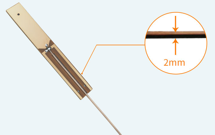
One of the popular methods for designing an antenna is to integrate it on the Printed Circuit Board (PCB) itself. This way, the antenna becomes an integral part of the PCB, and the system design becomes more compact and efficient. In this article, we will discuss the important aspects of designing an antenna on PCB Board.
1. Antenna Selection
Before designing an antenna on a PCB, we need to determine the type of antenna suitable for the application. The following are some popular types of antennas for PCBs:
- Microstrip Antenna
- Patch Antenna
- Meander Antenna
- Inverted F Antenna
- Dipole Antenna
Each type of antenna has its own unique advantages and disadvantages. The selection of the antenna type will depend on factors like frequency range, bandwidth, gain, size, and power handling capability.
2. Antenna Location and Layout
Once the antenna type is finalized, the next step is to determine its location and layout on the PCB. The key factors to consider here are:
- The proximity of the antenna to other components and traces on the PCB
- The orientation of the antenna with respect to the PCB and surrounding objects
- The clearance of the antenna from the edges of the PCB
It is advisable to keep the antenna away from other components and traces as much as possible to reduce interference and improve radiation efficiency. The orientation of the antenna should be such that it maximizes the signal strength in the desired direction. It is also important to maintain proper clearance around the antenna to avoid coupling with other elements.
3. Matching Networks
Impedance matching is a crucial aspect of antenna design. The impedance of the antenna should match the output impedance of the transmitter or receiver circuit to ensure maximum power transfer. If the impedance mismatch is significant, it can result in signal loss or distortion.
Matching networks like baluns, transformers, matching circuits, and capacitors can be added to the PCB to match the antenna impedance with the system impedance. The design of the matching network requires careful analysis and simulation to ensure optimal performance.
4. Routing and Grounding
The routing of traces and ground plane design on the PCB can also affect the antenna performance. The traces carrying the RF signals should be kept as short as possible to reduce losses due to transmission line effects. The ground plane should be designed to provide low impedance path for the RF signals and minimize the electromagnetic interference from other signals and noise sources.
5. Testing and Optimization
After the design is completed, the antenna should be tested and optimized for the desired performance. Various parameters like input impedance, return loss, radiation pattern, gain, efficiency, and bandwidth should be measured and compared with the design specifications. If the performance is not satisfactory, adjustments can be made in the design, matching network, or routing.
Conclusion
Designing an antenna on a PCB Board requires a deep understanding of the antenna theory, RF circuits, PCB design, and testing techniques. It is a complex and iterative process that requires attention to detail and careful analysis at every step. The final design should meet the desired specifications and ensure the best possible performance in the target application.
