PCB antenna anti-interference
With the proliferation of wireless communication technologies, radio frequency interference (RFI) has become a significant problem for designers of electronic devices. In this context, printed circuit board (PCB) antennas are increasingly being used in applications ranging from mobile phones to wireless routers. This article explains how to design a PCB antenna to be resistant to interference.
Reduce the Impact of Common-Mode Noise
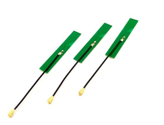
Common-mode noise is an electromagnetic wave that originates from sources outside the antenna, such as a natural or man-made noise source. It can cause unwanted electrical noise and distortion in the receiver electronics. There are several strategies that can help reduce the impact of common-mode noise on a PCB antenna.
First, it is possible to use a feed-line balun that isolates the antenna from external noise sources. The balun is connected to the antenna and the radio-frequency (RF) input, and is responsible for blocking common-mode noise that may interfere with the antenna's proper functioning.
It is also possible to match the impedance of the antenna to the RF circuitry by using an impedance-tuning network. This can help to reduce the impact of common-mode noise by making the circuit more resistant to external interference.
Finally, it is important to ensure that the PCB ground plane is properly connected to the antenna. This helps to reduce the impact of common-mode noise by providing a suitable path for current to flow.
Shield the Antenna
Another strategy for reducing the impact of RFI on a PCB antenna is to use shielding. This involves enclosing the antenna with a conductive material, such as copper foil or a metal mesh. The shielding is designed to block radio frequencies that may interfere with the antenna's operation, thus reducing the potential for electromagnetic interference (EMI).
It is also possible to use slot antennas as a way of shielding the antenna. Slot antennas consist of a conductive material with a slot cut in it, which can be positioned adjacent to the PCB antenna to form a shield. This helps to reduce the impact of RFI by redirecting stray electromagnetic waves away from the antenna.
Reduce Crosstalk
Crosstalk is the unwanted pick-up of signals from one circuit by another circuit. It can occur when two or more antennas are placed in close proximity to one another, or when the antenna is coupled with other electronic components on the PCB.
To reduce crosstalk, it is important to ensure that the antenna is isolated from other circuits on the PCB. This can be done by using a properly designed ground plane, which helps to isolate the antenna from other components.
Another strategy for reducing crosstalk is to use a high-quality RF connector that is designed to minimize interference. This can help to reduce the impact of crosstalk by minimizing the radio frequency leakage between the antenna and other components on the PCB.
Conclusion
Designing a PCB antenna to be resistant to interference requires a thorough understanding of the principles of electromagnetic radiation and the techniques used to minimize interference. By following the strategies outlined in this article, you can ensure that your PCB antenna is less susceptible to RFI and can operate more reliably in a range of applications.
